RAM expansion board
This page discusses how to expand the memory on a P2000T using modern chips. Want to grab a copy of the PCB files? Head directly over to the Github repository.
Background
Three variants of the P2000T were commercially sold with the labeling T/38, T/54 and T/102 which host 16, 32 and 80kb of RAM, respectively. There is also a variant with a PTC-floppyboard which can have both a 16k and a 64k memory expansion, yielding a total of 96k of RAM. The memory lay-out of the P2000T is organized as shown in the table below
| Address | Description |
|---|---|
| 0x0000-0x1000 | Monitor rom |
| 0x1000-0x4FFF | Cartridge |
| 0x5000-0x57FF | Video memory |
| 0x5800-0x5FFF | Unused |
| 0x6000-0x9FFF | RAM memory |
| 0xA000-0xDFFF | 16kb expansion |
| 0xE000-0xFFFF | 8kb banks |
For a T/38 model, the user could only access memory up to location
0x9FFF. The T/54 offered a 16kb expansion allowing the user to allocate
memory addresses 0xA000 - 0xDFFF. Finally, the T/102 model offered an
additional 64kb in comparison to the base model. Because the Z80 only has a
16 bit address register, bank switching was employed on the upper 8kb. By means
of writing a value between 0-5 to I/O address 0x94, the user could
select one of the 6 banks, each hosting 8 kb.
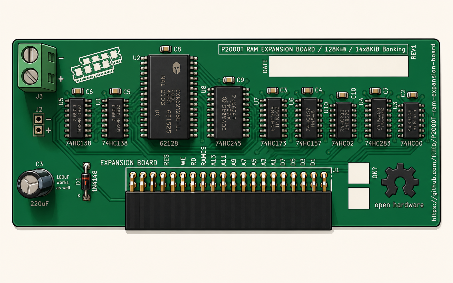
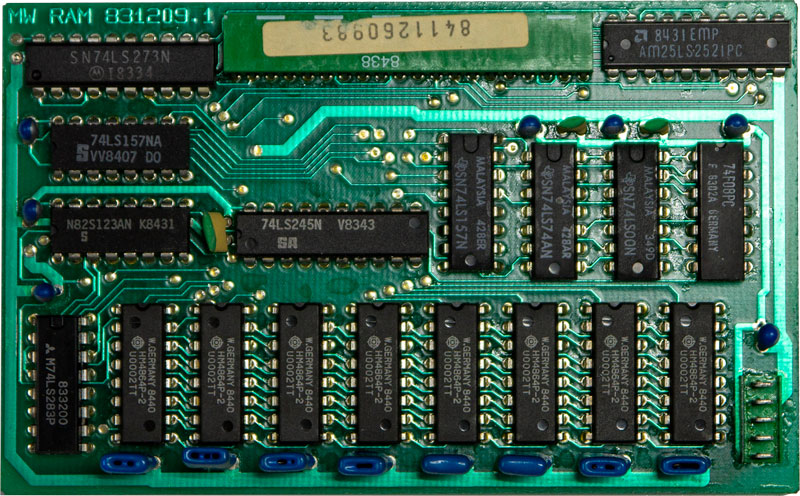
Expansion of the RAM was relatively easy (though expensive due to the cost of the DRAM chips back in the day) on a P2000T by means of inserting a small PCB onto the main board. A picture of such a board is shown in Figure 1.
Modern replica and features
The aim of the replica board is to provide a 64kb RAM expansion using modern chips
and employing static rather than dynamic memory. The board should monitor
I/O port 0x94 and accept read/write requests on that port to set a bank
register. Moreover, the board should adequately map the address lines between
the host P2000T system and the two 32kb memory chips taking the value of the
bank register into account. Finally, because we want to provide our venerable
P2000T with some reverse polarity protection which is accomplished by placing a
diode between the voltage input and the 5V rail on the RAM expansion board.
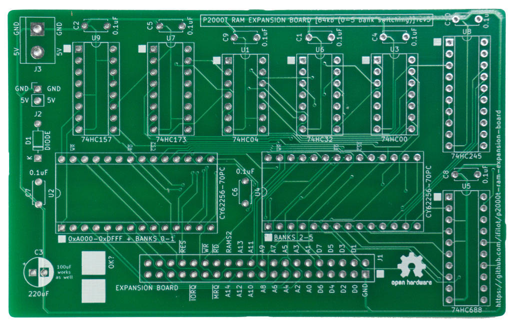
A full schematic of the PCB is provided in Figure 2.

Bill of materials
Besides the PCB, you will need the following components. It is recommended to use sockets for all the chips such that you can easily replace defective ones.
- 1x74HC00 (quad NAND-gate)
- 1x74HC04 (hex inverter)
- 1x74HC32 (quad OR-gate)
- 1x74HC157 (quad 2-input multiplexer)
- 1x74HC173 (quad positive edge triggered D-type flip-flop)
- 1x74HC688 (8-bit magnitude comparator)
- 1x74HC245 (octal bus transceiver)
- 2x62256 (32kb SRAM)
- 1x220uF capacitor (100uF also works)
- 8x0.1uF capacitor
- 1x1N4148 diode
- 1x 40 pin female pin header (2x20 pins; 2.54mm spacing)
- 1x screw terminal
Installation
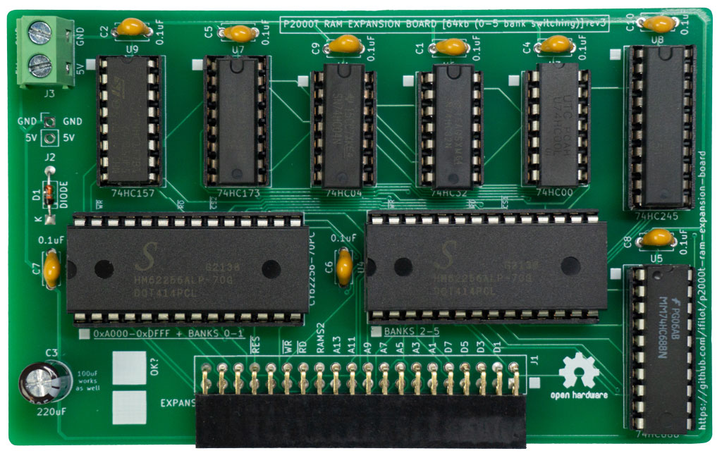
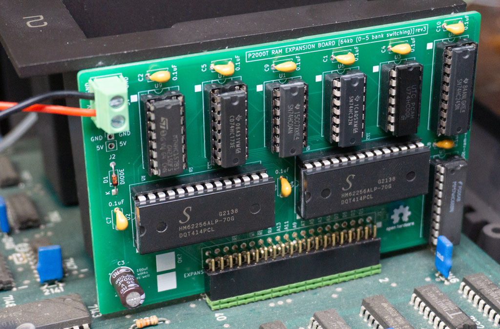
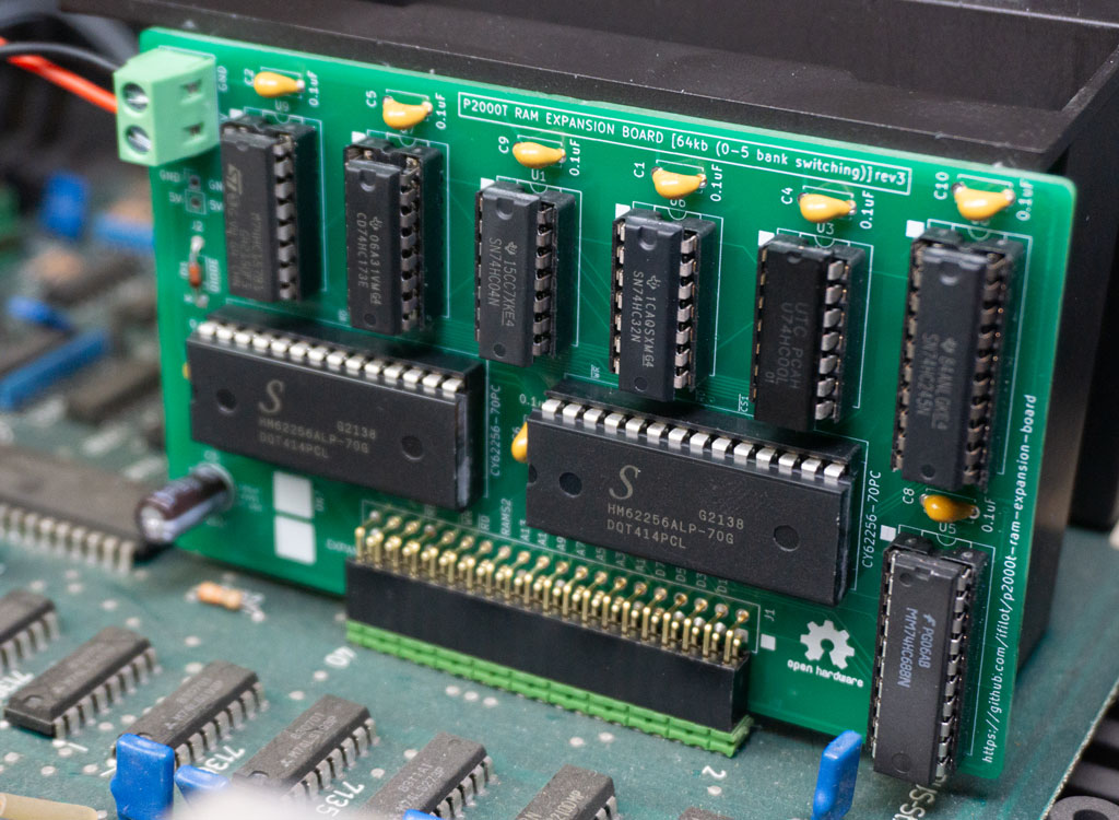
A photo of an unpopulated PCB is shown in Figure 3. Note that the 5V pins are indicated by a white square. Also note two big white squares next to C3. These can be used to write some check marks on the board with a sharpee. Soldering in all the components should be fairly easy to do by hand as all components are of the THT type.
A fully soldered and populated board should similar to the picture as shown in Figure 3. Before installing this board, always critically check the correct placement of all the chips. Since the current draw of modern chips is very low and because the board has reverse polarity protection, the chances that you will damage your P2000T upon a mistake is very small. That being said, if your P2000T does not boot properly after installing the board, immediately switch off the power and check the board carefully.
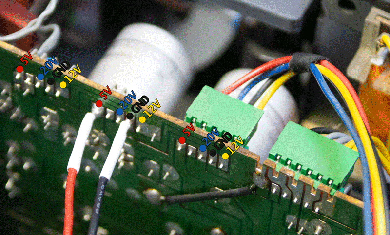
The memory expansion board is going to be fitted on the 40 pin male header on the backside of SLOT2. This 40 pin male header does not provide any 5V pin and as such we have to get this directly from the power PCB located next to the power transformer. The power PCB hosts four access points of which by default only the first two are in use. Each access point has 5 pins, corresponding to a 5V, a -22V, a 12V and two GND pins. Power is provided to your RAM expansion board by soldering two wires to the 5V and GND pins as shown in Figure 5. These wires will be connected to the terminal block on the RAM expansion board as shown in Figure 6 and Figure 7.
After soldering a GND and 5V wire onto the power PCB, connect these wires to the RAM expansion board using the screw terminal. Make sure the wires are properly fastened and cannot come loose.
Alternatively, you can also directly solder the wires onto the expansion board itself (there is an additional set of holes for that).
Next, mount the RAM expansion PCB onto the main board making sure the top sides of the chips are oriented away from SLOT2, as shown in Figure 6 and Figure 7
That is it. Place a BASIC ROM cartridge into SLOT1 and see if your P2000T properly boots. If not, immediately turn off the power and critically check all connections and chips. If it does boot up, the BASIC software should report near 40kb of free memory which is already an initial check that everything is working.
Testing
To test whether the RAM expansion board is properly functioning, one can either perform a simple test in BASIC or a more expansive test using a custom written memory testing utility. Both these procedures are explained below.
BASIC
If you want to test the bank switching functionality in BASIC, you can use the following instructions after booting the machine.
First, we need to set the top of BASIC to 0x9000.
CLEAR 50,&H9000
The reason we do this is to ensure that the stack is not residing at the
top 8kb because those bytes will become inaccessible after bank switching. Next,
we will first write a value to memory address 0xE000, check that this value
is properly written, change to another bank and read from the same memory address.
A different value should be returned (typically 0). Next, we write a different
value to the 0xE000 and change bank to the initial bank. The original value should
now be correctly retrieved. The procedure is performed using the following
snippet of BASIC code.
10 POKE &HE000,42
20 PRINT(PEEK(&HE000))
30 OUT &H94,1
40 PRINT(PEEK(&HE000))
50 POKE &HE000,43
60 OUT &H94,0
70 PRINT(PEEK(&HE000))
After entering in these instructions, type RUN. The output of this code should be
something similar to the code as shown below. The second value might be potentially
different, depending on earlier memory operations, though is expected to be a zero
on a fresh boot of the machine.
42
0
42
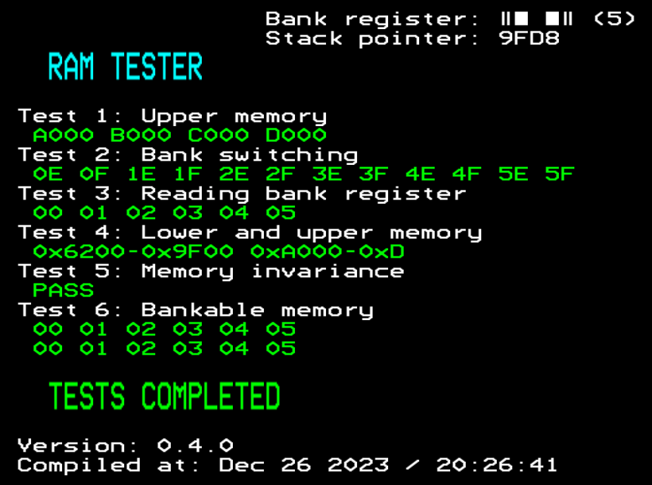
RAM testing cartridge
For a more extensive test of the memory, one can also make use of a dedicated memory testing cartridge. One needs however a writable cartridge such as the ZIF cartridge to perform such a test.
Download the latest version of the testing utility (RAMTEST.BIN) from the
releases page
and burn this file to a cartridge.
Insert the cartridge into SLOT1 and upon boot the RAM testing procedure will
automatically start. If the 64kb memory extension is working, all tests should
pass as shown in Figure 8.
Source files
All source files can be obtained from this Github repository. All source code, i.e. the ram tester utility, is released under a GPLv3 license. The hardware files (KiCad schematics) are released under the CC BY-SA 4.0 license.